Microscope for twistronics and spintronics studies
Patents for licensing
Researchers from the Nanophysics group, from the Department of Applied Physics at the University of Alicante, have developed a microscope whose structure and assembly allows twistronics and spintronics studies to be carried out jointly. Specifically, it allows the development of topography studies with atomic resolution, electronic transport studies and spin studies with the possibility of angular variation.
This invention, manufactured by 3D printing, stands out for its versatility, easy assembly, low price and adaptability to different experimental techniques.
The group is looking for companies or institutions interested in acquiring this technology for its commercial exploitation.

INTRODUCTION
Spintronics and twistronics are two research fields within nanoelectronics.
Spintronics is the emerging technology that uses both the electron's charge and its spin, while twistronics is defined as the novel science studying electronics as a function of the relative angle between two-dimensional layers. So far, the technical problem has been the impossibility, on the part of Scanning Tunneling Microscopes (STM), of studying these two fields together.
In this sense, within spintronics, the most useful devices in terms of both scientific and industrial production have been spin switches, which are devices capable of blocking or allowing spin transport.
To date, multiple forms of spin-switches that can be controlled under external stimuli, such as light, magnetic field or electric field, have been studied. However, there is no known spin-switch that adjusts its electrical conductance by a mechanical twist.
TECHNICAL DESCRIPTION
The invention consists of:
This new measuring instrument, a Scanning Tunneling Microscope (STM), has been manufactured using 3D printing, which allows its quick and easy development. Therefore, the construction process of the instrument consists of 3 steps: design, printing and assembly. First, 3D design software is used to design each individual part. Subsequently, the designs are exported to a printing software, with which the printing characteristics are configured and, finally, each part is printed separately. The assembly phase is based on the assembly of all the parts, as well as the manufacture of the parts and their wiring.
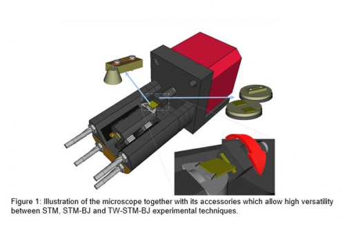
This assembled structure makes it possible to modify the working configuration by changing some parts mechanically, quickly and easily. By fixing more parts on the structure or on the front support, the configuration can be modified so that the same microscope can be used to develop the three different techniques, i.e. the standard STM technique, which allows topography images to be obtained on electrically conductive surfaces; the STM-BJ technique, with which electronic transport can be measured; and the Tw-STM-BJ technique, which allows the study of electronic and spintronic transport in a system whose electrodes are capable of rotating, and with which a spin-switch controlled by a rotation can be performed (see Figure 1).
MAIN ADVANTAGES OF THE TECHNOLOGY
The main advantages of this technology are the following:
INNOVATIVE ASPECTS
The structure of a Scanning Tunneling Microscope (STM) has been reinvented in order to carry out innovative twistronics and spintronics studies together. This microscope has been manufactured using 3D printing, which is a major advantage over non-standardised microscopes on the market.
The use of this manufacturing method allows it to be developed easily, quickly and accurately, as well as solving the problems of machining, standardisation and reproducibility of this type of instrument. Specifically, Polylactic Acid (PLA) has been used as a manufacturing material, which allows the microscope to be economical and sustainable, unlike current titanium microscopes.
As mentioned above, all previous studies in the field of twistronics have been based on two-dimensional overlapping slides, however, such a configuration does not allow for a controlled spin-switch with mechanical rotation. Therefore, this twistronics proposal, with electrodes facing each other at the edge, is totally innovative and clearly offers the possibility of controlling the relative angle between the electrodes to form a spin-switch.
CURRENT STATE OF DEVELOPMENT
Several prototypes of this microscope are already in operation in the Nanophysics group's own laboratory, as well as in other collaborating research centres such as Yachay Tech University or the National University of Costa Rica.
INTELLECTUAL PROPERTY RIGTHS
This technology is protected by patent application:
MARKET APPLICATION
It is primarily aimed at the nanoelectronics sector, more specifically, companies manufacturing tunneling microscopes (STM).
COLLABORATION SOUGHT
The group is looking for companies or institutions interested in acquiring this technology for commercial exploitation.
Ahead of the current Coronavirus outbreak, Innoget is fully committed to contributing to mobilizing scientific and expert communities to find a real solution to the Covid-19 pandemic. Therefore, we're supporting worldwide calls and programs that could help in any aspects of the coronavirus crisis.
Is your organization promoting or looking for innovation or research initiatives to mitigate the Covid-19 outbreak? Email us at covid19@innoget.com to list them.
Channeled through Innoget's online open innovation network, initiatives in the health, virology, medicine, or novel technologies applied to human health, among others, are listed and disseminated to Innoget members -ranging from hospitals, research institutes, scientists, businesses, and public administrations- and innovation partners worldwide.
Create your free account to connect with Universidad de Alicante and thousands of other innovative organizations and professionals worldwide
Send a request for information
to Universidad de Alicante
Technology Offers on Innoget are directly posted
and managed by its members as well as evaluation of requests for information. Innoget is the trusted open innovation and science network aimed at directly connect industry needs with professionals online.
Need help requesting additional information or have questions regarding this Technology Offer?
Contact Innoget support
