Multiple Stated Electrostatically Formed Nanowire Transistors (MSET)
Innovative Products and Technologies
Transistor-like device for the simplification of logical circuits. CMOS compaitable. Useful for FPGA. Also analogue.
Project ID : 9-2014-767

TECHNOLOGY
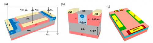
Electrostatically Formed Nanowires (EFN) based transistors have been recently suggested as robust sensing (Shalev et al. 2013) and memory devices (Shalev et al. 2012). The EFN device resembles the silicon-on-insulator (SOI) four gate field-effect transistor (G4-FET) developed in 2002 (Blalock et al. 2002) which emerged from the volume inversion SOI MOSFET. The G4-FET combines MOSFET and junction gate field-effect transistor (JFET) principles as it consists of a top MOS gate, a bottom substrate gate, and is located between by two lateral junction gates. The four gate transistor can be naturally adapted to CMOS technology scaling and manufactured in conventional silicon-on-insulator (SOI) processes with a low cost and high volume manufacturing. If a specific bias is applied to the side gates, the conduction band electrons between them are confined to a well-defined area forming a narrow conduction channel, the electrostatically-formed nanowire. Figure 1 (a) shows a schematic design of such a transistor. Figure 1 (b) illustrates the formation of the EFN in a cross section view.

Figure 1: 3D view of the 3 gate EFN transistor (a), cross section and formation of the EFN (b), 2 gates 2 drains MSET (c)
By applying non-symmetric bias on the side gates, the position of the EFN can be moved towards one of the gates (Shalev et al. 2013). We propose a novel Multiple State EFN Transistor (MSET) that exploits the EFN lateral movement in order to form a single transistor, multiple valued, multiplexer. In this device, the drain is split into several isolated individual drains and the MSET output is defined by a thin conduction channel between a specific drain and the source. Having a multiplexer functionality, this device can implement any logical operation within its inputs and outputs range. Since this device is based on simple SOI concepts, it can be integrated into current technology relatively easily. To the best of our knowledge, this is the first CMOS compatible transistor for MVL large-scale circuits to be suggested. A schematic illustration of an MSET device with two gates and two drains can be seen in Figure 1 (c).
THE NEED
As CMOS technology is expected to reach its fundamental limits in the near future, new logic and memory design concepts are subject of utmost importance. Multiple Valued Logic (MVL) can perform complex operations with a reduced number of transistors making it a natural candidate for replacing the current technology. Research on ternary logic (three-value logic) based on standard MOSFETs has been conducted in the 1980s. However, this technology was never been widely implemented. Resonant-Tunneling Bipolar Transistor (RTBT) and similar resonant-tunneling devices, particularly such with multiple negative differential resistance (MNDR) were also proposed as building blocks for MVL circuits. RTBT are three terminal heterojunction bipolar transistors and hence fundamentally different and not compatible with current CMOS technology. Furthermore, such devices are typically made of non-conventional elements, limiting their ability for wide spread implementation. Other MVL components have been realized with combined single electron and MOS transistors, bottom up grown nano-wires and Carbon Nano Tubes. However, to date it is unclear whether those can be integrated into large-scale circuit production.
POTENTIAL APPLICATION
The suggested device can be used as a basic building block for analog and digital circuits in Application Specific Integrated Circuits (ASIC) and Field Programmable Gate Arrays (FPGA). The combination of well defined conduction states and continuous gates voltages may make MSET based circuits attractive for mix signals (analog and digital) circuits such as digital to analog and analog to digital converters. If proved to have significant advantages over the common technologies in the three main criteria: Silicon area, Power consumption and Speed, the MSET technology can be used by all companies in the semiconductor industry. If MSETs are shown to have superior performance in part of the three parameters, they should be designated for use in specific products. For example, MSET based circuits that show superior low power consumption can be used in mobile applications.
STAGE OF DEVELOPMENT
The functionality of the devices was demonstrated with a semiconductor devices simulator. First prototypes were fabricated by TowerJazz and have demonstrated the basic MEST functionality. Optimized devices are currently being fabricated.
PATENTS
US | 8,007,727 B2 | Virtual semiconductor nanowire, and methods of using same | Aug 30, 2011 | Basic device has some similarites; Implementation for logic was not suggested. |
US | 8,241,913 B2 | Virtual semiconductor nanowire, and methods of using same | Aug 14, 2012 | Basic device has some similarites; Implementation for logic was not suggested. |
US | 8,318,505 B2 | Virtual semiconductor nanowire, and methods of using same | Nov 27, 2012 | Basic device has some similarites; Implementation for logic was not suggested. |
US | 8010591 B2 | Four-gate transistor analog multiplier circuit | Aug 30, 2011 | Basic analog function (multiplier) reialized with a 4 gates transisotr |
US | 2015/0017740 A1 | Molecular sensor based on virtual buried nanowire | Jan 15, 2015 | Basic device has some similarites; Implementation for logic was not suggested. |
WO2015181674A1 | Multiple state electrostatically formed nanowire Transistors |
SUPPORTING PUBLICATIONS
G. Segev, I. Amit, A. Godkin, A. Henning and Y. Rosenwaks, “Multiple State EFN Transistors”, Electron Device Letters, IEEE, 2015.