CNT-Based Structure for High-Resolution Semiconductor Process Control
Patents for licensing
With the continuous trend of electronic component miniaturization, process control technologies must keep up with component size reduction. Defects that were so far negligible, are now posing critical operation obstacles, and are more difficult to identify as scales are reduced to
The Need
The rapid advancements in electronics, including the ongoing miniaturization and increased structure complexity, require the development of supporting analysis techniques for failure detection to ensure device operation quality.
Of particular importance is the measurement of currents and potentials transferred through small structures and the detection of failure spots, particularly in buried structures. Among the most prevalent potential measurement methods are the Kelvin probe, which although has the advantage of being a non-contact device has a relatively low sensitivity, and the scanning tunneling microscope-based potentiometer that has higher sensitivity, yet requires the tunneling of electrons from the device under study and thus cannot be employed as a non-contact inspection method. Common devices for the detection of currents, such as the scanning SQUID and the Hall probe, suffer from relatively low measurement accuracy. No instrument enables the simultaneous detection of both currents and potentials.
The Solution
The proposed technology is based on a single-electron transistor (SET) made of carbon nanotubes (CNTs) which enables simultaneous visualization of both the currents and potentials of flowing electrons, eliminating the need to use several different instruments. It uses a non-contact approach that can accurately map information in buried structures even below an insulating layer, with sensitivity reaching three orders of magnitude higher than that of existing techniques. Its features render it suitable for high-sensitivity defect analysis in the microelectronic fabrication industry.
Technology Essence
The method takes advantage of the high voltage sensitivity of the scanning SET. It operates by applying a small AC bias voltage across a device of interest. The SET is used to isolate and image the potentials of the flowing electrons induced by the bias voltage. This can be done with a voltage imaging sensitivity of ~2uV/sqrt(Hz), three orders of magnitude (x1000) higher than that of the Kelvin probe technology, and can thus accurately map the potentials of flowing electrons. The current imaging sensitivity is ~10nA/um/sqrt(Hz) for semiconductors, which is X100 higher than that of SQUID-like techniques or scanning NV centers. As no charge is directly transferred between the SET and the device under study (unlike tunneling-based techniques), this method is ideally suited for high-sensitivity imaging potentials of flowing electrons in buried structures, which are increasingly prevalent. By applying a weak magnetic field perpendicular to the plane of the device, the SET can be used to map the local Hall voltage produced by flowing electrons, enabling imaging of the local current density. Unlike existing approaches, this method requires only local voltage measurements (instead of the global magnetic field), and is therefore less prone to artifacts. Imaging both the potential and current of flowing electrons relies on local voltage measurements, and can therefore be performed simultaneously, instead of requiring two separate apparatus/imaging tools.
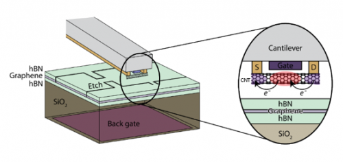
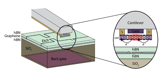
A schematic presentation of the arrangement of the carbon nanotube on the SET detection arm. The nanotube is connected to source and drain electrodes (yellow) and suspended above multiple gates (blue). The CNT structure is designed to scan the device of interest with no charge directly transferred between the probe and the inspected area.
Applications and Advantages
Advantages
Applications
Development Status
The group of researchers has demonstrated the validity of the invention on several graphene-based nanoscale devices (published in: Nature Nanotechnology, volume 14, 480–487 (2019) [1]). A series of experiments is planned to fully demonstrate the utility of the invention. A patent was granted for this invention and an additional patent application is pending.
Market Opportunity
According to a KPMG report from the “Global Semiconductor Industry Outlook 2019”, due to new developments, semiconductor production is becoming increasingly costly and “Increasing R&D costs” was flagged as the biggest issue facing the industry. The ongoing changes in the semiconductor fabrication industry require new, advanced inspection technologies that will keep up with the advancements in production technologies, reduce defect rates and maintain high yield. According to a recent report, the semiconductor inspection equipment market is estimated at $3.6 billion and is anticipated to increase at an 8.7% CAGR during 2019-2028. This evaluation is higher than the evaluated market increase in the broader semiconductor market, with a 6.9% CAGR during 2019-2024. This difference between expected market value of the inspection equipment and the broader semiconductor market further emphasizes the need for the development of novel production technologies and supporting defect analysis technologies. The value proposition of a novel, non-contact and high-resolution defect analysis technology, enabling maintained high production quality and yield in complex and reduced size chip structures is therefore obvious.
Yeda ("Knowledge" in Hebrew) Research and Development Company Ltd. is the commercial arm of the Weizmann Institute of Science (WIS) and is the second company of its kind established in the world.
WIS is one of the world’s leading multidisciplinary basic research institutions in the natural and exact sciences. It is located in Rehovot, Israel, just south of Tel Aviv. It was initially established as the Daniel Sieff Institute in 1934, by Israel and Rebecca Sieff of London in memory of their son Daniel. In 1949, it was renamed for Dr. Chaim Weizmann, the first President of the State of Israel and Founder of the Institute.
Yeda initiates and promotes the transfer to the global marketplace of research findings and innovative technologies developed by WIS scientists. Yeda holds an exclusive agreement with WIS to market and commercialize its intellectual property and generate income to support further research and education.
Since 1959 Yeda has generated the highest income per researcher compared to any other TTO worldwide. Weizmann has generated a number of groundbreaking therapies, such as Copaxone, Rebif, Tookad, Erbitux, Vectibix, Protrazza, Humira, and recently the CAR-T cancer therapy Yescarta.
Yeda performs the following activities:
◣ Identifies and assesses research projects with commercial potential.
◣ Protects the intellectual property of WIS and its scientists.
◣ Licenses WIS' inventions and technologies to industry.
◣ Establishes new Startup companies based in WIS Intellectual Property
◣ Channels funding from industry to research projects.
Our portfolio covers a broad spectrum of the natural sciences, including:
◣ Agriculture and Plant Genetics, including Bio-fuels
◣ Chemistry and Nanotechnology
◣ Environmental Sciences and Solar Energy
◣ Mathematics and Computer Science
◣ Medical Devices
◣ Pharmaceuticals and Diagnostics
◣ Physics and Electro-Optics
◣ Research Tools
Create your free account to connect with Yeda and thousands of other innovative organizations and professionals worldwide
Send a request for information
to Yeda
Technology Offers on Innoget are directly posted
and managed by its members as well as evaluation of requests for information. Innoget is the trusted open innovation and science network aimed at directly connect industry needs with professionals online.
Need help requesting additional information or have questions regarding this Technology Offer?
Contact Innoget support