 Yenny HernándezYenny Hernández
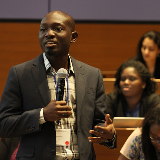 Jeffery AdadevohJeffery Adadevoh
 Hatice DabakHatice Dabak
 Hubert C MaxwellHubert C Maxwell
 Alex jiménezAlex jiménez Alexandros StavrinadisAlexandros Stavrinadis
Alexandros Stavrinadis
ICFO NEST Fellow at ICFO from Spain · Barcelona Area
I enjoy developing and understanding new materials that can improve existing technologies and create new ones. My current research is focused on semiconductor nanomaterials and thin films for optoelectronic applications like solar cells. I work on the synthesis and characterization of inorganic semiconductor and metallic thin films and nanoparticles. I use nanomaterials to make solar cells (photovoltaics) and other type of devices like thin film transistors (FETs) and photodetectors. Ultimately, I measure the efficiency and various optical and electronic properties of those devices and use the results as feedback to to innovate on and improve the conditions used during material growth and processing. Some material and thin film fabrication techniques I apply in my research are: -Physical Vapor Deposition (PVD) e.g. sputtering, thermal evaporation) -Thermal annealing processes i.e. rapid thermal annealing (RTP) -Colloidal synthesis of nanoparticles and quantum dots i.e. hot injection method -Sol-Gel i.e. for fabrication of oxide thin films In my work I use a number of material characterization techniques like -TEM, HREM, SAED, XRD, XPS, UPS, FT-IR, Raman, TGA, SEM, FIB, EDX, UV-Vis, PL, Cyclic Voltammetry Some of the most common optoelectronic measurements and analysis methods I utilize for understanding the physics of my semiconductor materials and devices are: -J-V characteristics under solar light -External quantum efficiency (EQE) measurements at short circuit and applied bias conditions -C-V characteristics and Mott-Schottky analysis -Transient photo- voltage and current (TPV, TPC) measurements -Stress and aging test of solar cells under various environmental conditions Some types of materials I am very familiar with are: -Quantum dots (e.g. PbS, CdS, PbSe) -Semiconductor Nanoparticles (e.g. Bi2S3, SnS) -Wide bandgap semiconductor films (e.g. ZnO, Ti2O) -Semiconductor polymers (e.g. P3HT, MEH-PPV). Adolfo GasparettoAdolfo Gasparetto
 Adi MesikaAdi Mesika
 DSADA DSADDSADA DSAD
 Jawad UllahJawad Ullah
 ignacio rodriguezignacio rodriguez
 dragana nikolovadragana nikolova
 Gabriel PérezGabriel Pérez
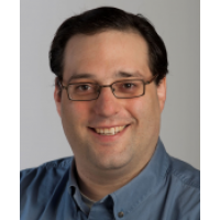 Elliot BiroElliot Biro
Elliot BiroElliot Biro is an Assistant Professor in the Department of Mechanical and Mechantronics Engineering. He has an extensive background in joining techniques used in the automotive and steel industries from his work with ArcelorMittal Global Research where he was responsible for many projects that applied metallurgical fundamentals to solve industrial problems. Dr. Biro’s experience includes process optimization for a variety of welding techniques (gas metal arc welding, spot welding, laser welding, high frequency induction welding, flash butt welding, and seam welding), understanding property changes and cracking during welding (heat affected zone softening and LME cracking), and development of simulation techniques to understand the metallurgical changes during welding and other steel manufacturing processes. Dr. Biro’s primary research interests are: metallurgical changes during welding, development of defects during welding, increasing process robustness to improve manufacturability, physical simulation of the welding process, welding of advanced high strength steels (AHSS), dissimilar material joining and weld evaluation. He currently sits on a variety of industry committees with the AWS and the CCIIW. From his work with industry Dr. Biro was responsible for $25M in savings to manufacturing costs from the results his projects and he has over 25 journal papers and 25 conference papers.
 Anish YadavAnish Yadav