 Alberto João Carvalho Sobrinho TeixeiraAlberto João Carvalho Sobrinho Teixeira
Alberto João Carvalho Sobrinho Teixeira
Innovation Manager at More - Research Mountains from Portugal · Bragança
With a degree in economics and a master's in marketing from the University of Coimbra, he specialized in territorial marketing in 2019. In the curriculum he has enough experience in internationalization processes for endogenous products, he was responsible for the internationalization process of the company Agromontesinho - Casa Agrícola de Vinhais , the biggest seller of Castanha and its derivatives in the municipality of Vinhais. As a collaborator at the Collaborative Laboratory MORE he is responsible for the Marketing department, where he has participated in several scientific and technological fairs. He is also responsible for the internationalization strategy of the laboratory, having developed contacts with several partner networks such as AICEP (Agency for Investment and Foreign Trade of Portugal) and AGRIFOOD digital innovation hub.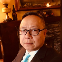
 The Economical Car Insurance Aurora ILThe Economical Car Insurance Aurora IL
The Economical Car Insurance Aurora ILOur aim is to serve the needs of car insurance for the residents of Aurora. The Economical Car Insurance Aurora IL can deliver the best professional advice and an insurance plan when you need it the most. The understanding of our team about your needs is something which makes us different from other organizations, give us a chance and witness the amazing experience of car insurance. Address :- 1331 Sheffer Road, Aurora, IL 60505 Tel No :- 331-204-1947 Website :- https://carinsuranceaurora.com/ Working Hours :- Mon To Sun - 9am–5pm
 Juan Carlos Gallardo HurtadoJuan Carlos Gallardo Hurtado
 The Reliable Car Insurance Joliet ILThe Reliable Car Insurance Joliet IL
The Reliable Car Insurance Joliet ILThe Reliable Car Insurance Joliet IL compared auto insurance rates in the city of Joliet, IL to identify the cheapest insurers and the rates they offer. The car insurance rates vary for a driver age / driver sex but the biggest impact on costs is variability in companies quotes. The highest quote in Joliet, IL, for example was $3,374 or 50% higher than the cheapest car insurance company’s quote of $2,808. This is exactly why we compel you should always get quotes from at least three companies so they can be compared. Use our form here to get multiple car insurance quotes at one place with just 4 one word questions answered, and that too instantly. Or you can call our local number 815 242 4616 to get instant car insurance quotes in Joliet, IL. Address :- 1551 Plainfield Rd, Joliet, IL 60435 Tel No :- 815-242-4616 Website :- https://carinsurancejoliet.com/ Working Hours :- Mon To Sun - Open 24 hours
 Jose Alberto Ochoa DisselkoenJose Alberto Ochoa Disselkoen
Jose Alberto Ochoa Disselkoen
Socio y Gte General at Tryger Ltda from Chile · Santiago
Desde 2002 a la fecha se ha especializado en la investigación y generación de nuevas tecnologías en áreas de la Ingeniería como: la naviera, salmonicultura, cultivo de chorito, Covid, pesca, alimentos marinos, eléctrica, residuos domésticos, basura internacional y otras creando y liderando nuevas empresas basadas en ellas. Todas estas tecnologías están debidamente patentadas. Jeff bastosJeff bastos
 mosa soedmosa soed
 Svetlana VolodaretsSvetlana Volodarets
 Imuzeze UsidameImuzeze Usidame
Imuzeze UsidameI am a technologist with a B. eng degree electrical engineering and electronics (1999) for 19 years of experience in the field of engineering. I have performed researches, carried out repairs and maintenance of diverse equipment in both electrical and electronic fields and mechanical engineering. I am self employed and conduct experiment for students in the field of electronics, measurement and control and electromechanical topics.
 Progressive Dental and AssociatesProgressive Dental and Associates
Progressive Dental and AssociatesAs a local dentist, Progressive Dental and Associates create lifelong relationships with our patients and their families and work to ensure that they receive treatments in a comfortable and relaxed environment. Dr. Durr and our staff invite you to schedule an appointment by calling 708-747-4294 and experience why our patients think Progressive Dental & Associates is the best dentist in Matteson. Address :- 20402 Crawford Ave #1, Matteson, IL 60443 Tel No :- 708-747-4294 Website :- https://www.progressivedentalsmiles.com/ Working Hours :- Mon -9am–6pm Tues to Thu - 8am-5pm Fri - 8am–2pm Sat-Sun Closed
 Antique Coins BuyersAntique Coins Buyers
 The Insurance LinkThe Insurance Link
The Insurance Link
business auto insurance san antonio at The Insurance Link from United States · San Antonio
The Insurance Link work on a customer centric working approach to analyze and fulfill customer demands. Our firm has been a champion in providing simplified administrative operations and reduced costs. As your Insurance service provider, we work to provide painless and easy open-enrollment, health benefits, health apps, and health cards using some of the best products on the market. We provide the customer service with more refined decision support. Address :- 15900 La Cantera Pkwy Ste. 20251, San Antonio, TX 78256 Tel No :- 210-776-7710 Website :- https://insurance-link.com/ Working Hours :- Mon To Fri - 9am–5pm